


Publikace
> Články v impaktovaných časopisech
> 'Processing and characterization of edgeless radiation detectors for large area detection'
Processing and characterization of edgeless radiation detectors for large area detection
Autor
| Kalliopuska Juha | VTT Technical Research Centre of Finland |
| Wu Xiaopeng | VTT Technical Research Centre of Finland |
| Jakůbek Jan, Ing. Ph.D. | UTEF |
| Eränen S. | VTT Technical Research Centre of Finland |
| Virolainen T. | VTT Technical Research Centre of Finland |
Rok
2013
Časopis
Nuclear Instruments and Methods in Physics Research A, Volume 731, p. 205-209
Web
Obsah
The edgeless or active edge silicon pixel detectors have been gaining a lot of interest due to improved silicon processing capabilities. At VTT, we have recently triggered a multi-project wafer process of edgeless silicon detectors. Totally SO pieces of 150 mm wafers were processed to provide a given number of detector variations. Fabricated detector thicknesses were 100, 200, 300 and 500 rim. The polarities of the fabricated detectors On the given thicknesses were n-in-n, p-in-n, n-in-p and p-in-p. On the n-in-n and n-in-p wafers the pixel isolation was made either with a Common p-stop grid or with a shallow p-spray doping. The wafer materials were high resistivity Float Zone and Magnetic Czochralski silicon with crystal orientation of < 100 >. In this paper, the electric properties on various types or detectors are presented. The results from spectroscopic measurement show a good energy resolution of the edge pixels, indicating an excellent charge collection near the edge pixels of the edgeless detector.
Granty
Projekty
Příklad citace článku:
J. Kalliopuska, X. Wu, J. Jakůbek, . Eränen, T. Virolainen, "Processing and characterization of edgeless radiation detectors for large area detection", Nuclear Instruments and Methods in Physics Research A, Volume 731, p. 205-209 (2013)
Hledat
Události
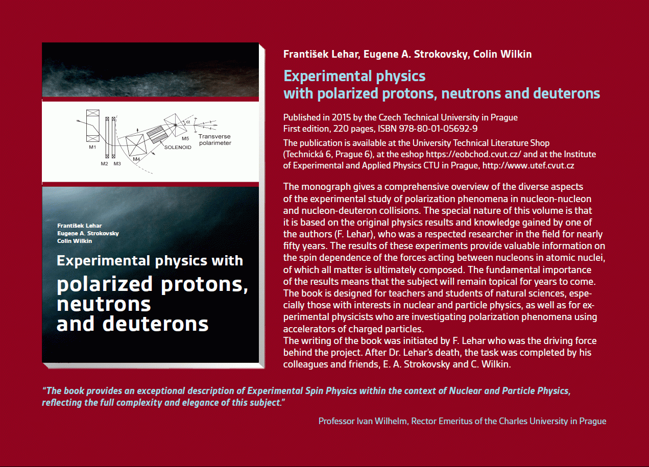 Experimental physics
with polarized protons, neutrons and deuterons
Experimental physics
with polarized protons, neutrons and deuterons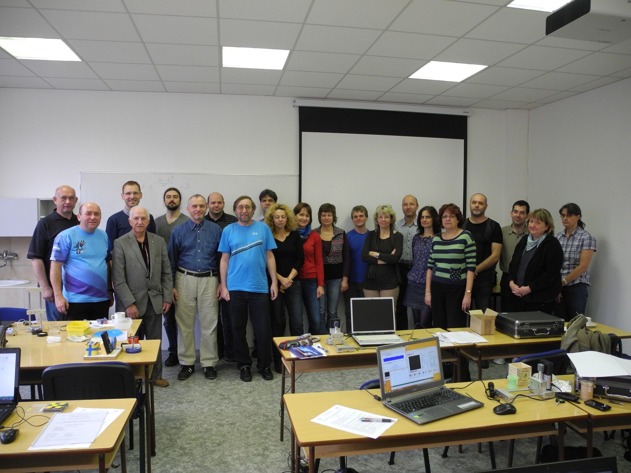 Progresivní detekční metody ve výuce subatomové a částicové fyziky
na ZŠ a SŠ
Progresivní detekční metody ve výuce subatomové a částicové fyziky
na ZŠ a SŠ21.-22. 11. 2014
 NSS MIC IEEE Conference
Seattle, USA
8-15 Nov 2014
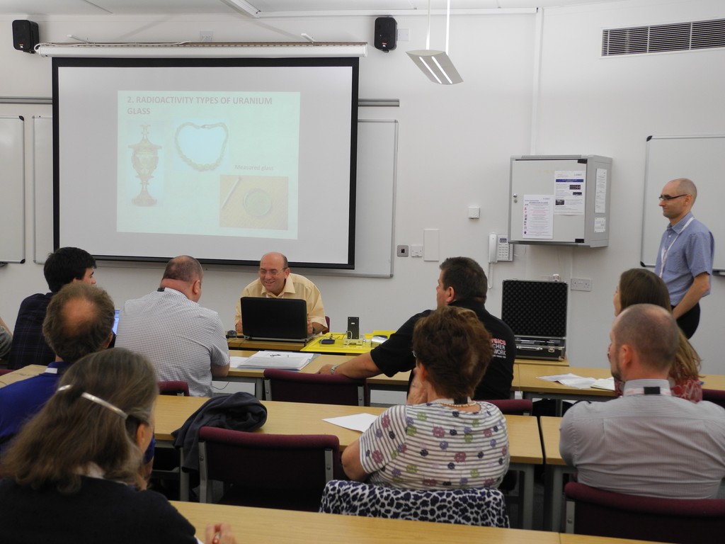 Konference SEPnet, CERN@school
Surrey, Velká Británie
8. září 2014
 Lovci záhad - spolupráce ČT a ÚTEF
9. září 2014
 Progresivní detekční metody ve výuce subatomové a částicové fyziky na ZŠ a SŠ
24. 4. 2014
 Návštěva v rámci projektu „Listening to the universe by detection cosmic rays“
3. 4. 2014
Seoul, Korea
27 Oct - 2 Nov 2013
 15thIWORID
Paris
23-27 June 2013
 NSS MIC IEEE Conference
Anaheim, USA
29 Oct - 3 Nov 2012
