


Semináře
> Microelectronics Technology for Integrated Semiconductor Pixel Detectors
Microelectronics Technology for Integrated Semiconductor Pixel Detectors
Datum
3.5.2011 14:00
Přednášející
| Erik Heijne | CERN, NIKHEF, ÚTEF ČVUT v Praze |
Obsah
In a typical pixel detector using submicron CMOS technology one is now able to integrate in each microscopic pixel a traditional nuclear electronics readout chain, including ADC and data storage. However, the technology is approaching 10nm dimensions for active elements, and one can dream of more complicated integration. Will this allow to create new systems for scientific studies ? Probably one needs to integrate also adjacent technological developments in miniaturization of actuators and microfluidic cooling. The current approach to nanoelectronics is based on mass production with very expensive lithographic masks. For scientific applications, alternatives are becoming very much needed.
Hledat
Události
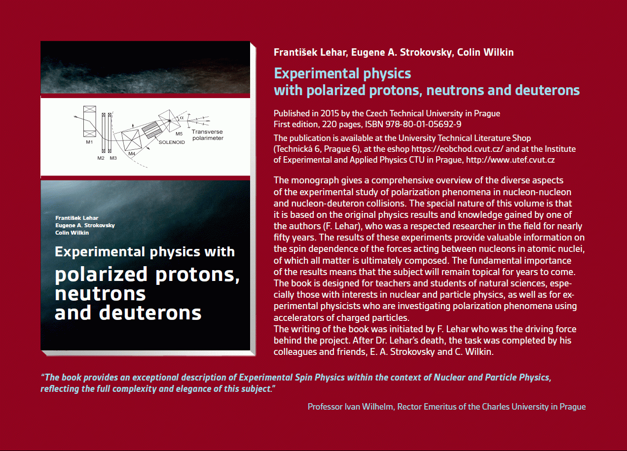 Experimental physics
with polarized protons, neutrons and deuterons
Experimental physics
with polarized protons, neutrons and deuterons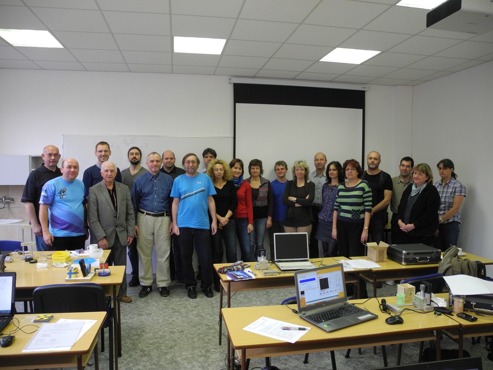 Progresivní detekční metody ve výuce subatomové a částicové fyziky
na ZŠ a SŠ
Progresivní detekční metody ve výuce subatomové a částicové fyziky
na ZŠ a SŠ21.-22. 11. 2014
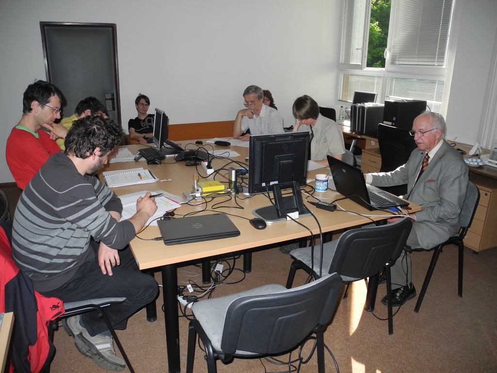
 NSS MIC IEEE Conference
Seattle, USA
8-15 Nov 2014
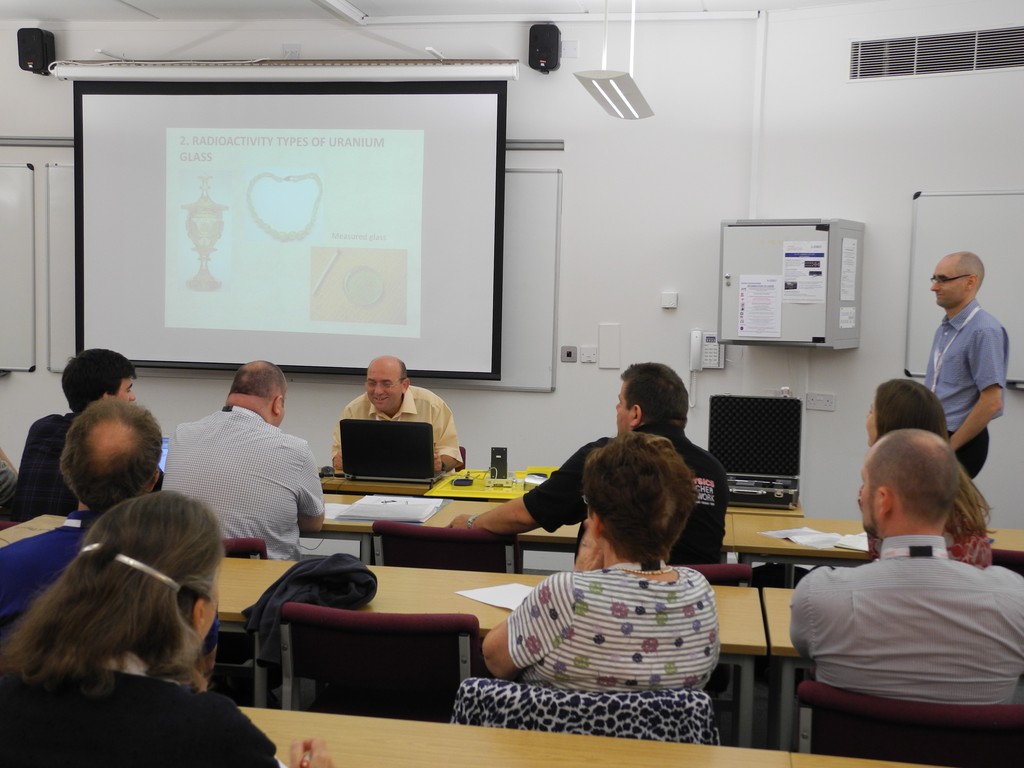 Konference SEPnet, CERN@school
Surrey, Velká Británie
8. září 2014
 Lovci záhad - spolupráce ČT a ÚTEF
9. září 2014
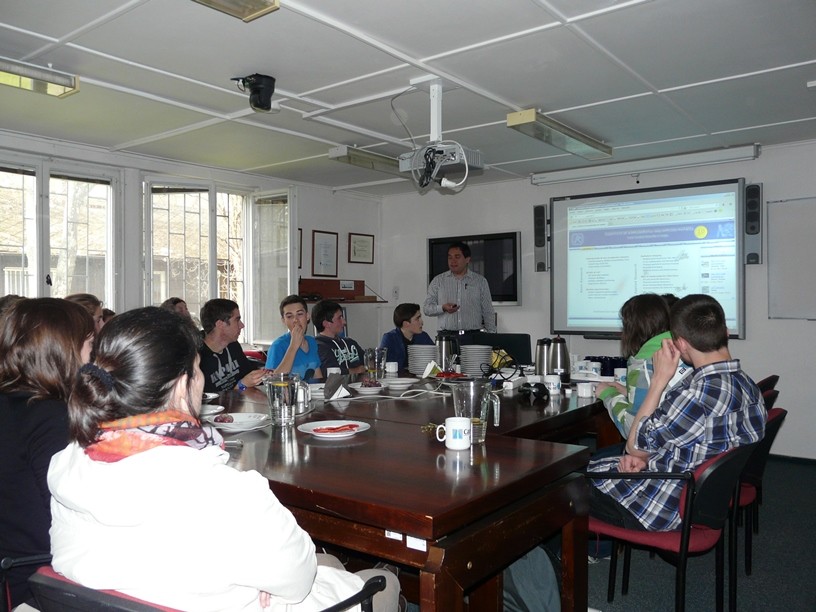
 Progresivní detekční metody ve výuce subatomové a částicové fyziky na ZŠ a SŠ
24. 4. 2014
 Návštěva v rámci projektu „Listening to the universe by detection cosmic rays“
3. 4. 2014
Seoul, Korea
27 Oct - 2 Nov 2013
 15thIWORID
Paris
23-27 June 2013
 NSS MIC IEEE Conference
Anaheim, USA
29 Oct - 3 Nov 2012
