


Publikace
> Články v impaktovaných časopisech
> 'Probe and scanning system for 3D response mapping of pixelated semiconductor detector with X-rays and the timepix device'
Probe and scanning system for 3D response mapping of pixelated semiconductor detector with X-rays and the timepix device
Autor
| Jakůbek Martin, Ing. | UTEF |
| Jakůbek Jan, Ing. Ph.D. | UTEF |
| Žemlička Jan, Ing. | UTEF |
| Kroupa Martin, Ing. | UTEF |
| Krejčí František, Ing. | UTEF |
Rok
2012
Časopis
AIP Conf. Proc. 1423, pp. 461-466; doi:10.1063/1.3688846
Web
Obsah
The development of new radiation detectors of different semiconductor materials (Si, CdTe, GaAs, …) brings the necessity to test and evaluate their response and detection performance such as the spatial homogeneity and local charge collection efficiency. A number of these materials exhibit a certain degree of inhomogeneity, which is needed to be determined in order to eliminate its negative effects. Similarly, such testing is desired as well in order to determine the extent of radiation damage in detectors. We decided to build a size-configurable beam and detector positioning system to probe the collection of charge spatially localized deposited by X-rays on a pixelated detector. The principle of this system is based on the use of a collimated parallel X-ray beam with a line profile, which delivers a defined charge at a specific location in 3D in the sensor. The beam can be sent onto the pixelated sensor at a low angle, which allows determining, for a given angle and detector position, the depth of interaction for each pixel. Shifting the detector along the axis perpendicular to the plane of the beam we can obtain a map of the detector response which is in 3D—i.e. both across the sensor plane and along its depth. Per-pixel signal read out from the pixelated detector can be done by usage of the hybrid semiconductor device Timepix which allows per-pixel energy measurement. The Timepix chip contains an array of 256×256 square pixels (total over 65 k pixels) with pitch size 55 μm. Our method allows probing and scanning the collection of charge at different depths across the pixelated sensor. Moreover, it allows determining the effect of radiation damage at μm scale. All these effects can be studied as well in the dependence on various detector parameters such as the sensor bias voltage. Results with a specific detector are presented.
Granty
Příklad citace článku:
M. Jakůbek, J. Jakůbek, J. Žemlička, M. Kroupa, F. Krejčí, "Probe and scanning system for 3D response mapping of pixelated semiconductor detector with X-rays and the timepix device", AIP Conf. Proc. 1423, pp. 461-466; doi:10.1063/1.3688846 (2012)
Hledat
Události
 Experimental physics
with polarized protons, neutrons and deuterons
Experimental physics
with polarized protons, neutrons and deuterons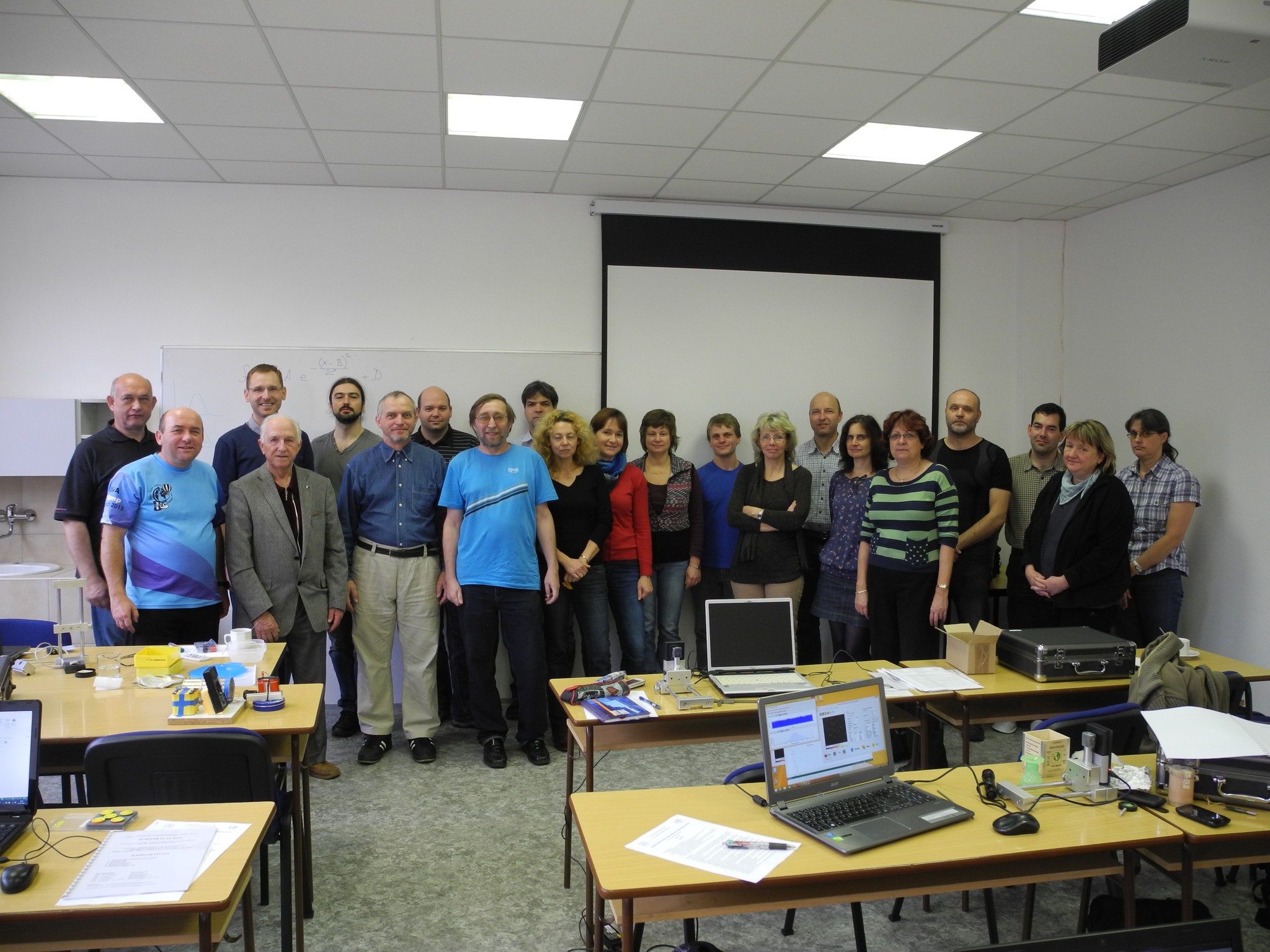 Progresivní detekční metody ve výuce subatomové a částicové fyziky
na ZŠ a SŠ
Progresivní detekční metody ve výuce subatomové a částicové fyziky
na ZŠ a SŠ21.-22. 11. 2014
 NSS MIC IEEE Conference
Seattle, USA
8-15 Nov 2014
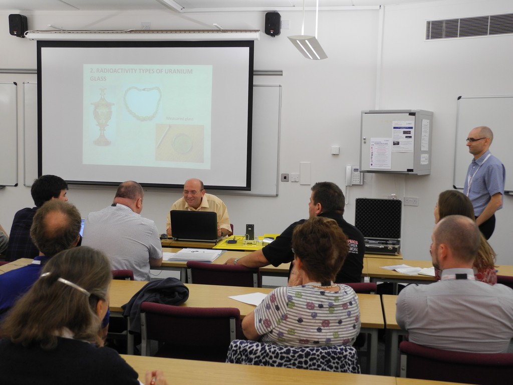 Konference SEPnet, CERN@school
Surrey, Velká Británie
8. září 2014
 Lovci záhad - spolupráce ČT a ÚTEF
9. září 2014
 Progresivní detekční metody ve výuce subatomové a částicové fyziky na ZŠ a SŠ
24. 4. 2014
 Návštěva v rámci projektu „Listening to the universe by detection cosmic rays“
3. 4. 2014
Seoul, Korea
27 Oct - 2 Nov 2013
 15thIWORID
Paris
23-27 June 2013
 NSS MIC IEEE Conference
Anaheim, USA
29 Oct - 3 Nov 2012
