


Publication
> Articles in Impacted Journals
> 'Processing and characterization of edgeless radiation detectors for large area detection'
Processing and characterization of edgeless radiation detectors for large area detection
Author
| Kalliopuska Juha | VTT Technical Research Centre of Finland |
| Wu Xiaopeng | VTT Technical Research Centre of Finland |
| Jakůbek Jan, Ing. Ph.D. | IEAP |
| Eränen S. | VTT Technical Research Centre of Finland |
| Virolainen T. | VTT Technical Research Centre of Finland |
Year
2013
Scientific journal
Nuclear Instruments and Methods in Physics Research A, Volume 731, p. 205-209
Web
Abstract
The edgeless or active edge silicon pixel detectors have been gaining a lot of interest due to improved silicon processing capabilities. At VTT, we have recently triggered a multi-project wafer process of edgeless silicon detectors. Totally SO pieces of 150 mm wafers were processed to provide a given number of detector variations. Fabricated detector thicknesses were 100, 200, 300 and 500 rim. The polarities of the fabricated detectors On the given thicknesses were n-in-n, p-in-n, n-in-p and p-in-p. On the n-in-n and n-in-p wafers the pixel isolation was made either with a Common p-stop grid or with a shallow p-spray doping. The wafer materials were high resistivity Float Zone and Magnetic Czochralski silicon with crystal orientation of < 100 >. In this paper, the electric properties on various types or detectors are presented. The results from spectroscopic measurement show a good energy resolution of the edge pixels, indicating an excellent charge collection near the edge pixels of the edgeless detector.
Grants
Projects
Cite article as:
J. Kalliopuska, X. Wu, J. Jakůbek, . Eränen, T. Virolainen, "Processing and characterization of edgeless radiation detectors for large area detection", Nuclear Instruments and Methods in Physics Research A, Volume 731, p. 205-209 (2013)
Search
Recent events
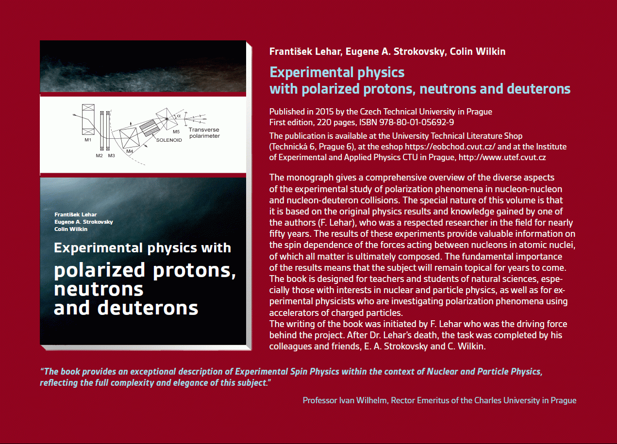 Experimental physics
with polarized protons, neutrons and deuterons
Experimental physics
with polarized protons, neutrons and deuterons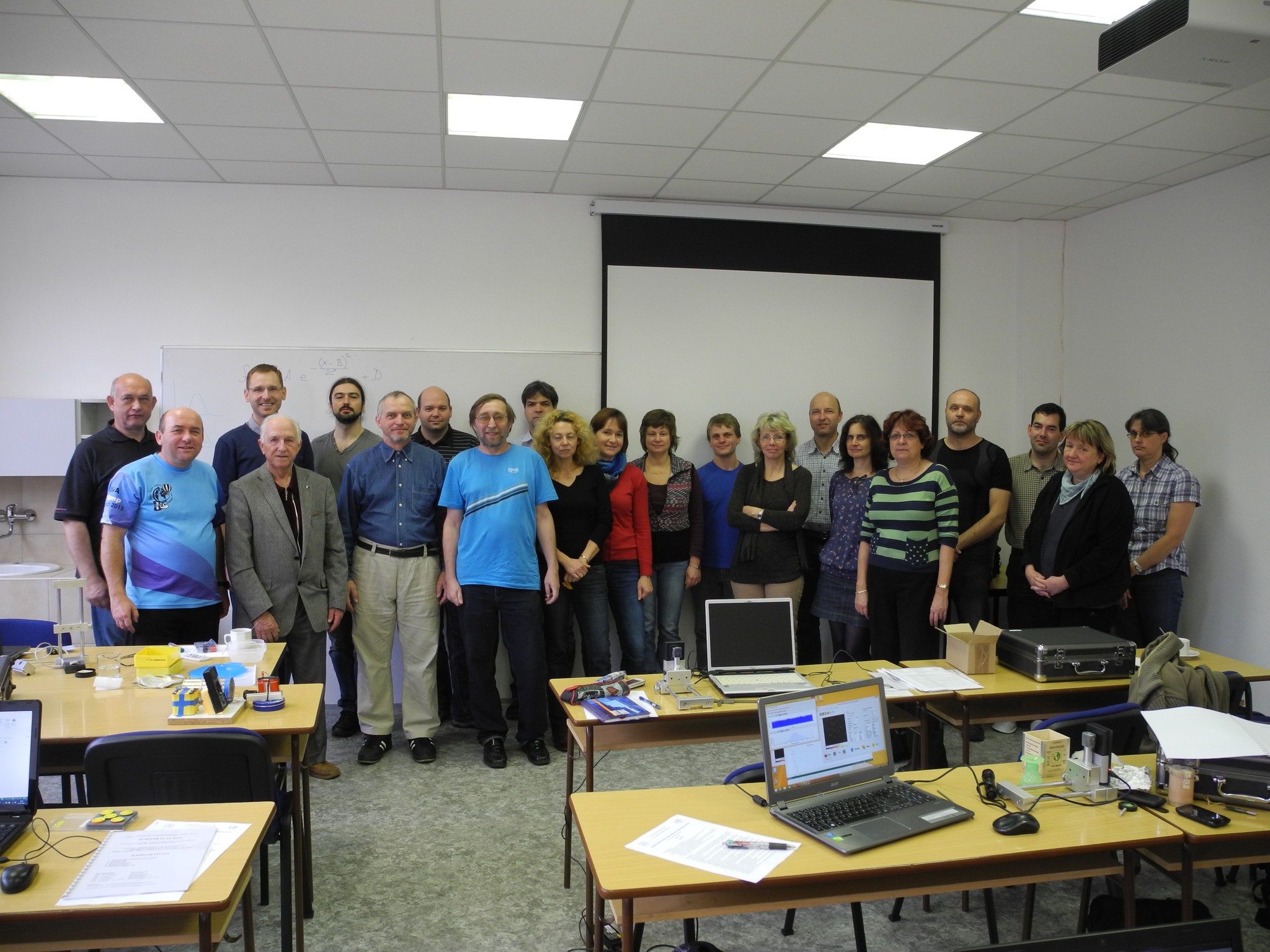 Progressive detection methods in atomic and particle physics education at middle and high school level
 NSS MIC IEEE Conference
Seattle, USA
8-15 Nov 2014
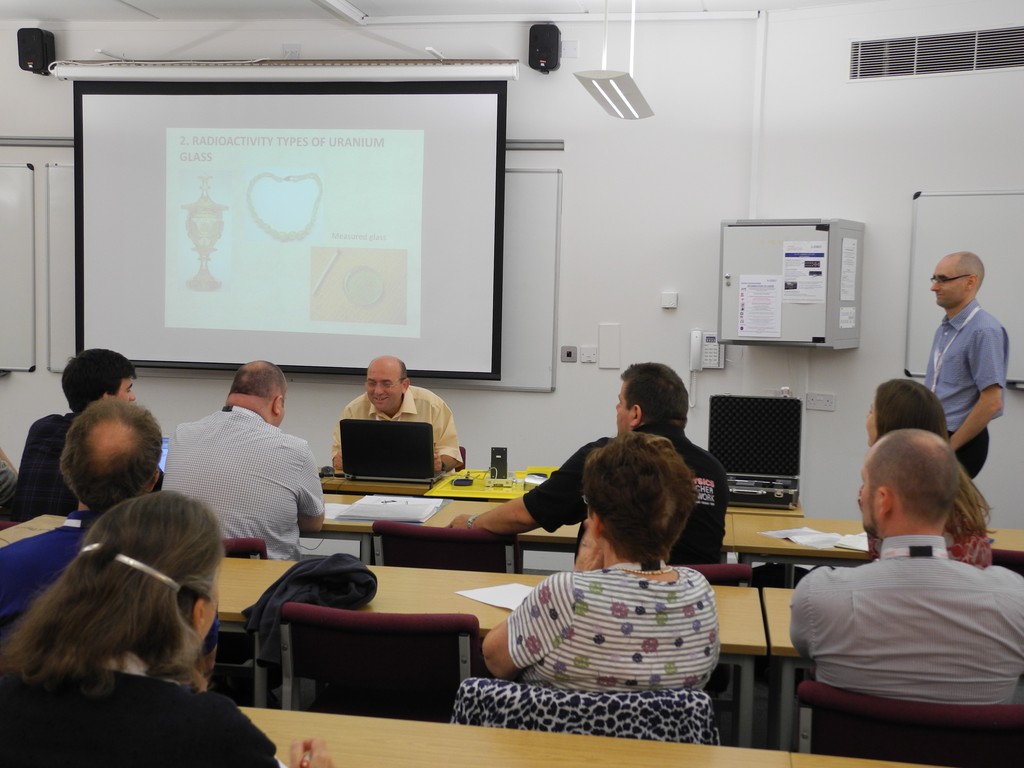 SEPnet, CERN@school Conference
Surrey, United Kingdom
Sep. 8, 2014
 Lovci záhad - natáčení ČT ve spolupráci s ÚTEF
 Advanced detection methods in atomic and subatomic physics education.
April 24, 2014
 Listening to the universe by detection cosmic rays - visit of French and Czech students
3 Apr 2014
Seoul, Korea
27 Oct - 2 Nov 2013
 15thIWORID
Paris
23-27 June 2013
 NSS MIC IEEE Conference
29 Oct - 3 Nov 2012
