


Goal:
- Provide the possibility of defined radiation damage of semiconductor samples at high flows of fast neutrons.
- Ensure the calibration method of verification of radiation damage dose.
The principle of radiation damage
Radiation damage of semiconductor detectors is result of local generation of crystal structure defects. The word "defect" is generally used as a shorter synonym for the word "imperfection". Defect can be any deviation from the ideal crystalline grid in the case of crystals, or any deviation from the ideal random chain in the case of amorphous substances. Defects caused by radiation damage are the result of interaction of particles of ionizing radiation with individual atoms of the substance. Defect in the form of interstitial atom and vacancy arises when particle transmits to atom sufficient amount of energy to leave its original location in the crystal grid (e.g. 25 eV in the case of silicon). Due to thermal vibrations of grid these defects can travel, interact a form defective multiple systems (clusters). Defects can also travel to its original position in the crystal grid. Radiation damage is changing over time. This phenomenon is called the effect of annealing. Furthermore, although less likely, may be caused defects in type of impurity elements other than that the substance is initially composed. Example of the cause of such defect can be nuclear transmutation.
What causes radiation damage
Defects caused not only by radiologic damage can create in a restricted band levels which may be occupied by charge carriers (or on which can be free charge carriers catched and subsequently released). Defects therefore strongly influence the electrical and detection properties of crystals, such as conductivity of the crystal and charge collection efficiency. The detailed study and careful description of physical phenomena caused by defects allows the correct identification of these defects. This will help identify the improvements in the design technology of semiconductor detectors, so that these detectors have better characteristics required (e.g. to be more radiation-resistant).
| Linhart Vladimir | IEAP |
(7)

 Year
Year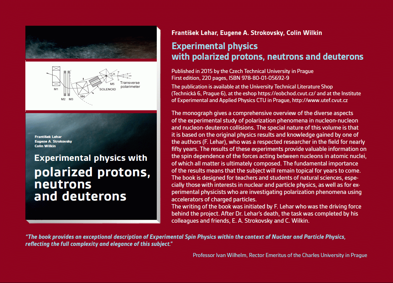 Experimental physics
with polarized protons, neutrons and deuterons
Experimental physics
with polarized protons, neutrons and deuterons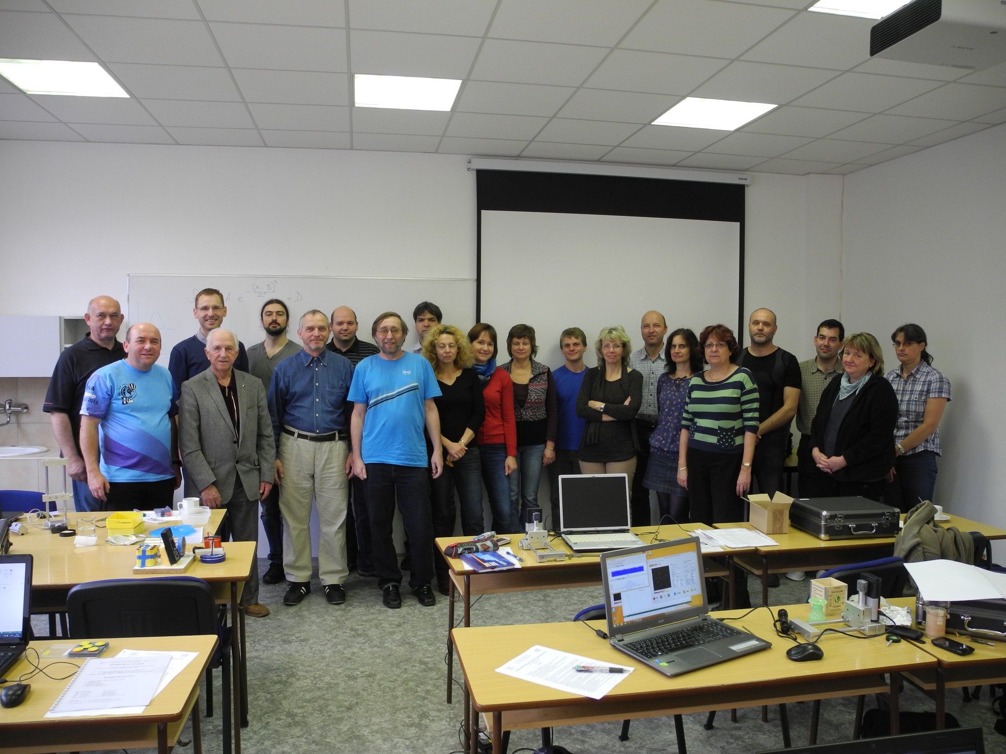 Progressive detection methods in atomic and particle physics education at middle and high school level
 NSS MIC IEEE Conference
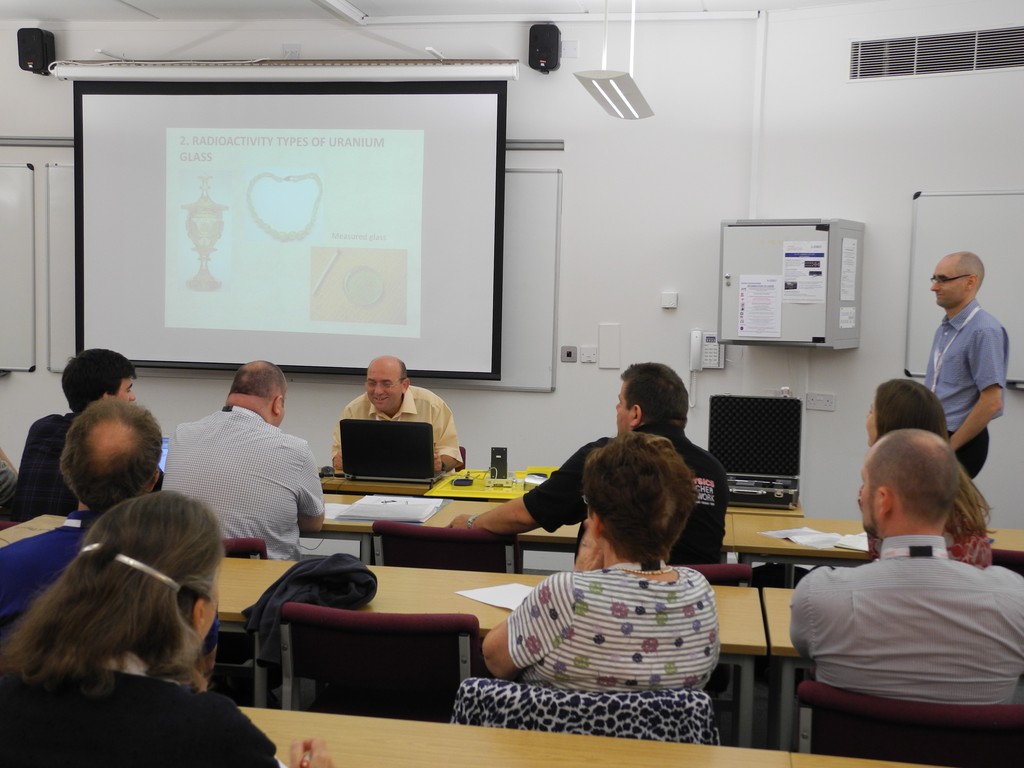 SEPnet, CERN@school Conference
 Lovci záhad - natáčení ČT ve spolupráci s ÚTEF
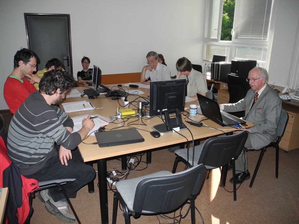 Advanced detection methods in atomic and subatomic physics education.
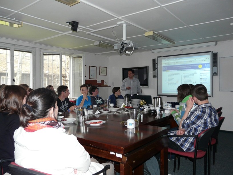 Listening to the universe by detection cosmic rays - visit of French and Czech students
 15thIWORID
 NSS MIC IEEE Conference