


Goal:
In cooperation with leading research institutions to develop new types of semiconductor detectors, to provide complex tests of the widest possible family of semiconductor detectors, and improve the physical description of their behavior.
Why do we deal with semiconductor detectors?
The main advantage of semiconductor detectors, compared to gas detectors, is their higher detection efficiency (associated with higher density) and better spectrometric resolution (associated with less energy needed to create one electron-hole pair). Our main concern is promoting the use of semiconductor detectors and their spectrometric characteristics.
In short about semiconducting detectors
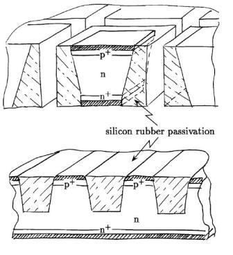
Development of semiconductor detectors was allowed by technological development allowing the cultivation of sufficient clean mono-crystals (typically Si and Ge) and creation of various detection structures (conventional diodes, heterogeneous junctions, strips, pixels ...). It has been shown that for detectors is the best to use a plate cut from semiconductor mono-crystal and to create transitions and electrodes directly on the crystal. This can be created by planar technology developed by Jean Honernim and Robert Noyce at Fairchild Semiconductor in 1959. This technology, originally developed for low-cost and rapid production of electronic components (transistors, integrated circuits ...), allows diffusion of different impurities into semiconductor bulk and etching different structures. Detectors manufactured by this technology are generally known as planar detectors . Their specific names, however, are often based on the shape of the collection electrodes. Pad detectors are planar detectors in form of ordinary diodes, i.e., thin plate of mono-crystal extrinsic semiconductor (e.g. N type) where on one side is created metalized rectifying transition (e.g. Schotky contact, PN transition, MIS structure or heterogeneous junction) and on the other side, is created ohmic transition. Strip detectors (e.g. ATLAS SCT modules) are made similar to pad detectors, but the rectifying transition (including metal) is divided into parallel or slightly divergent strips. Pixel detectors (e.g. Medipix) are segmented to pixels where each pixel may play a role of one picture.
Use of planar technology, however, has certain limitations. These restrictions are dictated by the fact that planar technology allows adjustment of only the surface of semiconductors and only just in layers parallel with the surface. Planar technology, therefore, cannot enlarge the active area surface of a semiconductor detector (magnification such areas should achieve an increase in detection efficiency of detector with a conversion layer on the surface). Thickness of planar detectors is limited by distance, on which can free charge carriers drift in electric field for the duration of their life. Typical thickness of detectors such as: 20 mm (Ge detectors), 2 mm (CdTe detectors), 0,3 mm (Si detectors), 0.2 mm (InP and GaAs detectors). Current research is therefore focused on the suppression of these constraints through improved technology, e.g. electro-chemical etching. Detectors manufactured by this technology are called 3D and Semi-3D detectors.
(11)

| Name | Author | Scientific journal |  Year Year
|
| Radiation hardness properties of full-3D active edge silicon sensors | Da Viá C.; Hasi J.; Kenney C.; Linhart V.; Parker S.; Slavíček T.; Watts S.; Bém P.; Horažďovský T.; Pospíšil S. | NIM A 587 (2008) 243–249 | 2008 | |
| Characterization of 3D thermal neutron semiconductor detectors | Uher J.; Jakůbek J.; Kohout Z.; Linhart V.; Pospíšil S.; Fröjd C.; Petersson S.; Kenney C.; Parker S.; Thungstrom G. | NIM A 576 (2007) 32-37 | 2007 | |
| Composite polycrystalline boron nitride for alpha and neutron detectors | Schieber M.; Linhart V.; Zuck A.; Roth M.; Marom G.; Khakhan O.; Pospíšil S. | JOURNAL OF OPTOELECTRONICS AND ADVANCED MATERIALS Vol. 9, No. 6, June 2007, p. 1746 - 1749 | 2007 | |
| Efficiency of composite boron nitride neutron detectors in comparison with helium-3 detectors | Uher J.; Pospíšil S.; Linhart V.; Schieber M. | APPLIED PHYSICS LETTERS 90, 124101 (2007) | 2007 | |
| Modified Hecht model qualifying radiation damage in standard and oxygenated silicon detectors from 10MeV protons | Charbonnier A.; Charron S.; Houdayer A.; Lebel C.; Leroy C.; Linhart V.; Pospíšil S. | NIM A 576 (2007) 75–79 | 2007 | |
| Role of electrode metallization in performance of semi-insulating GaAs radiation detectors | Dubecký F.; Boháček P.; Sekáčová M.; Zaťko B.; Lalinský T.; Linhart V.; Mudroň J.; Pospíšil S. | NIM A 576 (2007) 87–89 | 2007 | |
| Etched trenches in technology of monolithic strip detectors based on semi-insulating GaAs | Perďochová- Šagátová A.; Dubecký F.; Nečas V.; Linhart V. | NIM A 563 (2006) 74–77 | 2006 | |
| Experimental analysis of the electric field distribution in GaAs radiation detectors | Perďochová- Šagátová A.; Linhart V.; Dubecký F.; Zaťko B.; Nečas V.; Pospíšil S. | NIM A 563 (2006) 187–191 | 2006 | |
| Measurements of fast-neutron-induced signals in pad detectors | Linhart V.; Bém P.; Gotz M.; Honusek M.; Pospíšil S.; Šimečková E. | NIM A 563 (2006) 263–267 | 2006 | |
| Radiation damage study of GaAs detectors irradiated by fast neutrons | Linhart V.; Bém P.; Gotz M.; Honusek M.; Mareš J.; Slavíček T.; Sopko B.; Šimečková E. | NIM A 563 (2006) 66–69 | 2006 | |
| Development of radiation tolerant semiconductor detectors for the Super-LHC | Moll M.; Chren D.; Horažďovský T.; Kohout Z.; Linhart V.; Pospíšil S.; Sopko B.; Sopko V.; Uher J.; et al. | NIM A 546 (2005) 99–107 | 2005 |
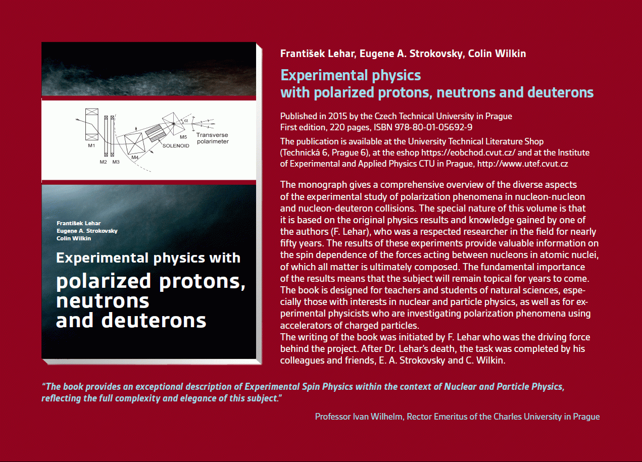 Experimental physics
with polarized protons, neutrons and deuterons
Experimental physics
with polarized protons, neutrons and deuterons Progressive detection methods in atomic and particle physics education at middle and high school level
 NSS MIC IEEE Conference
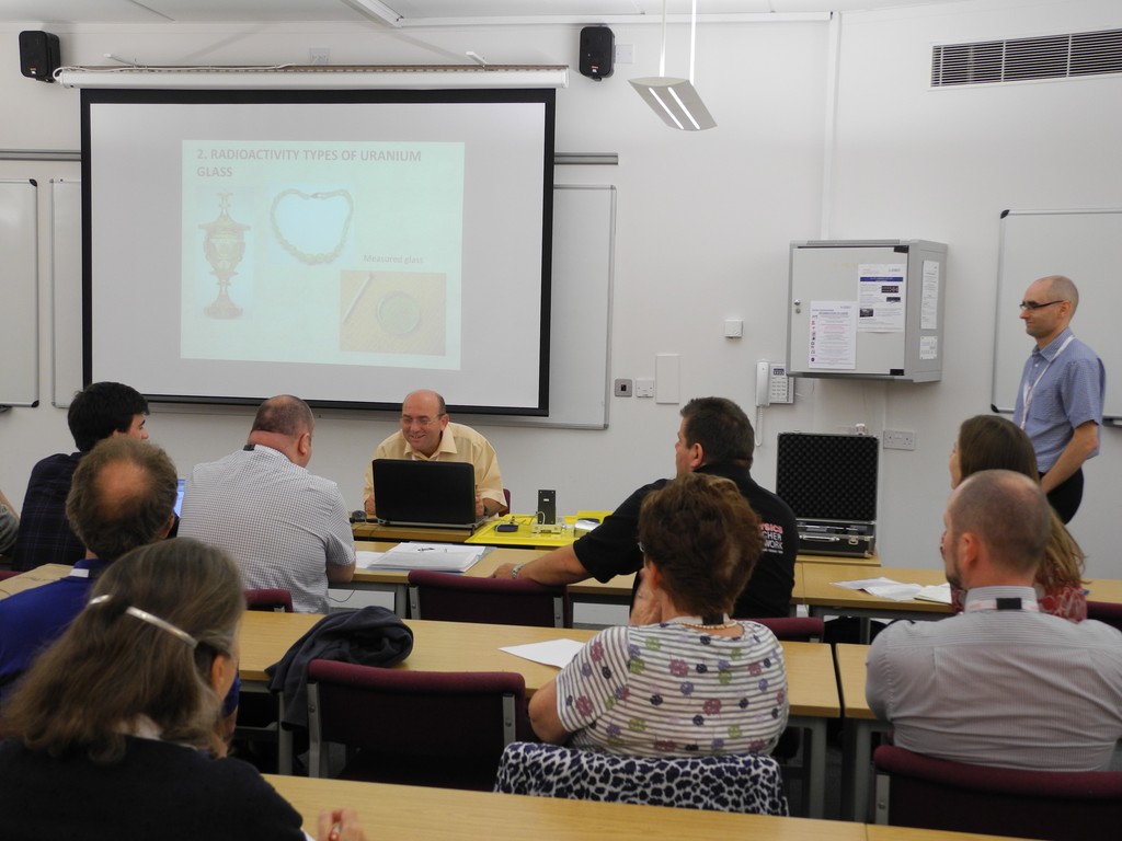 SEPnet, CERN@school Conference
 Lovci záhad - natáčení ČT ve spolupráci s ÚTEF
 Advanced detection methods in atomic and subatomic physics education.
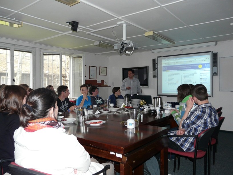 Listening to the universe by detection cosmic rays - visit of French and Czech students
 15thIWORID
 NSS MIC IEEE Conference